Spintronics: The classical manipulation of electronic spin.
As an alternative to electronic charge, the storage and transport of electronic spin in semiconductor devices - “spintronics”, may revolutionize the electronic device industry, with spin based transistors , opto-electronic devices, and memory. Moreover, the ability to preserve coherent spin states in conventional semiconductors and quantum dots may eventually enable quantum computing in the solid state. Although efficient room temperature electrical spin injection in metals has been commercially employed into today’s magnetic read heads through giant magnetoresistance, electrical spin injection into semiconductors has been quite challenging.
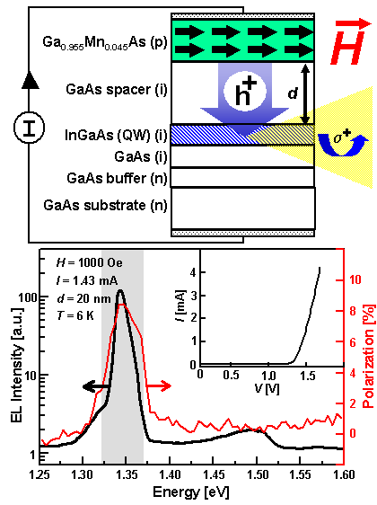
In this experiment we fabricate all-semiconductor, light-emitting spintronic devices using III-V heterostructures based on GaAs, where electrical spin injection occurs in zero magnetic field from a ferromagnetic semiconductor into a non-magnetic semiconductor. Under forward bias, spin polarized holes from the p-type ferromagnetic semiconductor (Ga,Mn)As and unpolarized electrons from an n-type GaAs substrate are injected into an embedded (In,Ga)As quantum well (QW) separated from the ferromagnetic region by a spacer layer. The hole spin polarization in the QW is directly measured by analyzing the polarization of the emitted electroluminescence (EL). Total EL intensity of the device under forward bias at T = 6K and H = 1000 Oe is shown (black curve) with its corresponding polarization (red curve). Note that the polarization is largest at the QW ground state (E = 1.34 eV). A current-voltage (I-V) characteristic of a 20nm spacer layer device is shown in the inset.
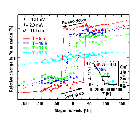
Hysteretic EL polarization is a direct result of spin injection from the ferromagnetic (Ga,Mn)As layer. The main panel shows relative changes in the energy-integrated (shaded gray area in spectra above) polarization DP, at temperatures from T = 6-52 K, as a function of in-plane field from a device with d = 140 nm. In the inset, we plot the relative remanent polarization, (DP at H = 0 Oe) shown in solid squares between T = 6 -94 K along with the temperature dependence of the (Ga,Mn)As magnetic moment, measured by a SQUID magnetometer (solid black curve), demonstrating that polarization is proportional to magnetic moment.
The presence of hysteretic polarization observed in magnetic samples with d = 20-220 nm, and its absence in the control samples, indicates that hole spins can be injected and transported over 200 nm. This occurs in spite of possible depolarization due to transport through interfaces, as well as valence band mixing in the bulk and QW regions. The demonstration of electrical spin injection into a semiconductor, especially in the absence of an applied magnetic field, opens a variety of new technological opportunities including electrical control of magnetization, integration of nonvolatile storage and logic, and manipulation of quantum spin states in semiconductors.
To learn more about this measurement, see:
"Electrical Spin Injection in a Ferromagnetic Semiconductor Heterostructure", Y. Ohno, D.K. Young, B. Beschoten, F. Matsukura, H. Ohno and D.D. Awschalom, Nature, vol. 402, p. 790 (1999)