The spin coherence of individual nitrogen vacancy (NV) centers in diamond makes them an exceptional candidate for quantum information processing applications. The demonstration of room temperature millisecond NV center spin coherence times has motivated many proposals for coherently coupling NV center spins via dipole interactions and for coupling single NV center spins to other systems such as photonic crystals, superconducting resonators, and magnetic cantilevers. However, because the electric and magnetic dipole fields associated with a single spin are very small nearly all of these proposals require NV center placement on ~10 nm length scales to achieve proximal coherent coupling. To generate this defect-based spin system on these length scales we have developed a nanofabrication technique based on patterning nitrogen ion implantation in diamond with electron beam lithography masks. By creating a mask of nanoapertures in electron beam lithography resist we are able to template the implantation of nitrogen ions into a high-purity diamond substrate. After removing the resist mask we then anneal the samples at a temperature such that the vacancies in the diamond lattice created by the nitrogen implantation diffuse to the implanted nitrogen atoms to form nitrogen vacancy centers.
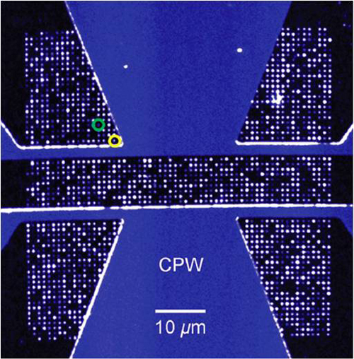
This nanofabrication technique offers both high spatial resolution for NV center formation and high throughput: resist apertures are scalable to 10 nm diameters and 30 nm pitches and can be fabricated at a rate of ~103 apertures per second. A photoluminescence image of an array of NV centers formed by this technique is shown below; the white dots correspond to NV center luminescence while formerly masked areas of the sample show no photoluminescence. In this example the patterned apertures were ~60 nm in diameter and were implanted with a broad-beam nitrogen ion dose of 1 x 10¹² nitrogen/cm2. The diffuse white lines seen on the sample surface come from a metallic stripline lithographically fabricated on the diamond for spin resonance measurements. Two single NV centers, confirmed by photon antibunching measurements, are circled in the image. In this array on average about 1.5 NV centers formed per aperture.
We have also further characterized our system using secondary ion mass spectroscopy (SIMS) and electron spin resonance (ESR) measurements. SIMS measurements facilitated depth profiling of the implanted nitrogen to provide three-dimensional characterization of the NV center spatial distribution. These measurements demonstrated that low energy ion implantation, in combination with careful orientation of the nitrogen ion beam relative to the diamond crystallographic planes, can generate NV centers at the shallow depths necessary for NV center coherent coupling schemes. The ESR measurements of single nanofabricated NV centers showed coherence times on the order of 10 μs, short relative to the longest coherence times demonstrated for NV centers in high-purity diamond. This is likely a result of the current low creation efficiency of NV centers in these implanted samples. In the example image shown roughly 30 nitrogen ions were implanted per aperture to form on average 1.5 NV centers per aperture. Future work will focus on improving the coherence and creation efficiency of these implanted NV centers through optimized annealing and implantation procedures to leverage the high NV center spatial resolution demonstrated in this work for the creation of coherent multi-qubit NV center devices.
To learn more about our studies, please refer to "Chip-Scale Nanofabrication of Single Spins and Spin Arrays in Diamond", D. M. Toyli, C. D. Weis, G. D. Fuchs, T. Schenkel, and D. D. Awschalom, Nano Lett. 10, 3168 (2010).
Related article: "Diamond Feats Give Quantum Computing a Solid Boost", Science 329, 616 (2010).