The neutral divacancy in the 4H polytype of silicon carbide (SiC) is an optically addressable spin-1 system that has been proposed as a useful spin-qubit platform due to it near-infrared optical emission and long spin lifetimes in its groundstate. Unfortuntately, due to SiC's low Debye-Waller factor, which governs how often a photon will be emitted from the divacancy at a predictable frequency without coupling to a phonon excitation in the crystal, this system suffers as a single photon emitter that can be utilized for robust and fast entanglment generation that will be necessary for quantum internet infrastructure. The higher the Debye-Waller factor, the more photons that carry the spin-qubit's information are emitted at the zero phonon line (ZPL) frequncy of the divacancy.
One way to increase the ZPL emission is to construct a high quality factor optical cavity around the divacancy defect that changes the amount of the photons that are emitted at a different wavelength. The enhancement of ZPL emission is commonly described by the Purcell factor, which quantifies an excited state's lifetime reduction as a ration of emission rates.

Γ_cavity and Γ_bulk are the cavity-enhanced and unmodified emission rates of the divacancy. F = 1 defines no enhancement and typical values that utilize good cavities range from ~4 to several hundred. Next, λ_cavity is the resonant wavelength, and n is the index of refraction. Q is the quality factor and V is the mode volume of the photonic cavity. Finally, The terms F1 and F2 represent spatial overlap and spectral matching between the emitter and cavity mode, respectively.

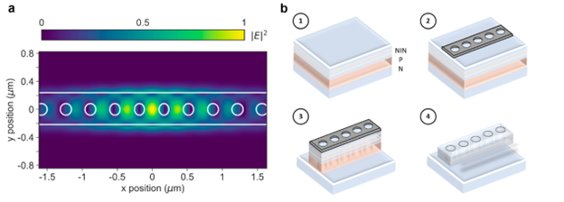
This work utilizes a combination of nanolithography and a dopant-selective photoelectrochemical etch process to produce suspended cavities with quality factors exceeding 5000, as seen in the photoluminescence spectrum taken at room temperature. A Purcell enhancement, F, of approximately 50 is observed for a single axial (inset: a missing carbon and silicon atom oriented along the c-axis of 4H-SiC) divacancy defect emitter found to exist inside the nanobeam cavity structure. Also, control of the divacancy ground-state spin is also characterized.

The 1D nanobeam structure photonic cavity is composed of a suspended section of SiC with elliptical holes along its length that taper to circles away from the center to trap the light around a region (a) where defects will be measured that undergo Purcell enhancement due to interaction with the strong fields inside the cavity. Electron beam lithography defines the in-plane patterning and then a selective etching process is used to undercut the beams. Silicon carbide has the advantage as a semiconductor that can be purchased from commercial growers as epilayer stacks with varying p-type or n-type dopants. Specifically, an photoelectrochemical etch followed by HF bath etches away the p-type layer (b, orange layer) after the surrounding SiC is removed.

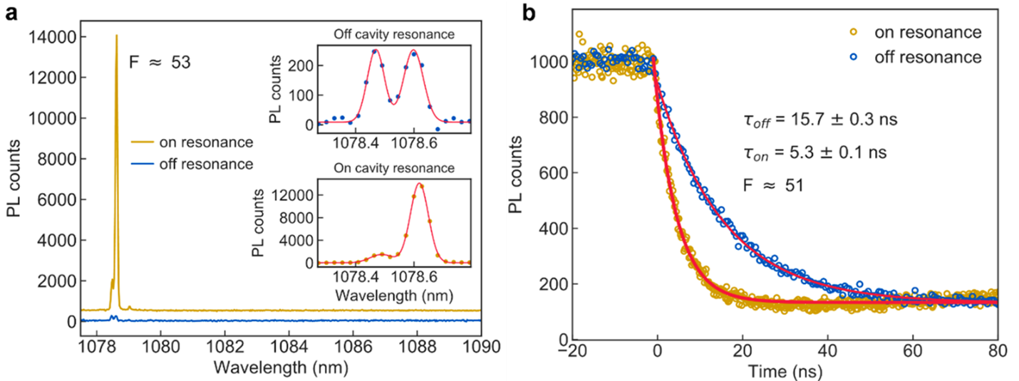
The results for observing Purcell enhancement of a single divacancy within the nanobeam cavities is shown above. An emitter inside one of the beams at a temperature of 5 K was confirmed with photoluminescence excitation (PLE) scans, optical detected magnetic resonance (ODMR), and a g(2) autocorrelation measurement to be an hh species of divacancy. The inset in (a) shows that when the emitter is addressed with off-resonant 905 nm light, while the cavity is on resonance with the PLE excitation line near 1078.6 nm, there is a dramatic increase in the measured photons corresponding to an increase in the ZPL counts. The Purcell factor was extracted to be ~ 53. In a similar experiment, using laser light on resonance with that same transition, the excited state life time was measured to be around 3x shorter when on resonance with the cavity, givening similar Purcell factor.
The last experiment involved measuring the coherence of a prepared spin state in the divacancy both inside and outside the photonic crystal cavity. The measured inhomogeneous dephasing time (T2*) for a state prepared in the magnetic ground state sublevels was seen to be 4x larger if measured on a defect not in the cavity. This indicates the proximity of the defect to the etched walls of the nanobeam structure has a large impact on its ability to act as a spin-register. Sources of dephasing include proximity to trapped surface charges or large strain due to crystal damage. Improved etching processes or post-etch surface treatment could improve the spin coherence quality. As a whole, this system advances the prospects of spin-to-photon transduction for the neutral divacancy in entanglement schemes and other quantum information applications.
Details can be found in our manuscript: