Although quantum-mechanical phenomena such as entanglement and coherence may seem non-intuitive or even ‘spooky’ to some, these phenomena can actually be manipulated in a highly controlled manner in certain laboratory settings. One example is the nitrogen-vacancy (NV) center in diamond (structure illustrated below), which is a defect in the diamond crystal lattice that traps electrons and confines them to a very small region of space within the crystal. Because of the particular manner in which these electrons are confined, their total spin (a quantum-mechanical trait of the electrons that behaves like tiny magnetic moment) can be initialized, coherently manipulated, and measured using light and microwave radiation, all at room temperature and on an individual defect-by-defect basis.

This makes the NV center in diamond an excellent candidate for a qubit, the basic unit of a quantum computer. A quantum computer is a proposed computing device that would exploit entanglement and coherence in order to solve certain computational problems more quickly than is currently possible with the computers of today that rely on traditional Boolean logic. However, much like the first commercial microprocessors that incorporated thousands of transistors on one semiconducting die, a practical and general quantum computer will need to contain many thousands of individual qubits, which must, in turn, be able to interact with one another on command via an information bus.
Although the quantum-mechanical properties of the NV in diamond have made it a leading candidate for the qubits of tomorrow’s quantum processors, it is currently difficult to grow or fabricate devices from diamond crystals. Additionally, the diamond NV is just one of an enormous number of crystalline defects found in nature, very few of which have been characterized to a high degree. Therefore, in the effort to build a defect-based quantum computer, it is essential to explore the quantum physics of defects more fully and to search for other defects with NV-like properties.
We are currently searching for defects analogous to the diamond NV, but in other wide-bandgap semiconductors. Because the list of potential defects and host materials is so large, a systematic way of singling out the most promising candidates for future study is necessary. In order to intelligently sort through potential defect qubit candidates, we have developed a set of physical criteria that a defect and its host material should satisfy in order to possess functionality similar to that of the NV in diamond. General physical arguments relating the electronic structure of defects to their atomic structure can then be used in conjunction with computational tools to evaluate whether a given defect satisfies the criteria we have put forth.
For instance, the energies of a defect’s electronic traps (relative to one-another and to the energies of the host material’s band edges) play a major role in determining whether a defect can meet the criteria we put forth. But the energies of these levels are related to the geometry and atomic composition of the defect and its surrounding host. As illustrated below for the case of vacancy-impurity complexes in tetrahedrally-coordinated semiconductors, four spin-degenerate electronic levels are possible within the bandgap, due to the four dangling bonds of the atoms surrounding the vacancy. Furthermore, the electronic levels of anion vacancies will tend to be located more closely to the valence band, while those of cation vacancies will tend to be closer to the conduction band (panel A). While the levels of a naked vacancy will exhibit one splitting due to the interactions among the dangling bonds of the surrounding four atoms (panel B - ΔAV and ΔCV), a second splitting will occur in a vacancy-impurity complex because the impurity will have a dangling bond energy different than that of its three neighbors (panel C - δAV and δCV).
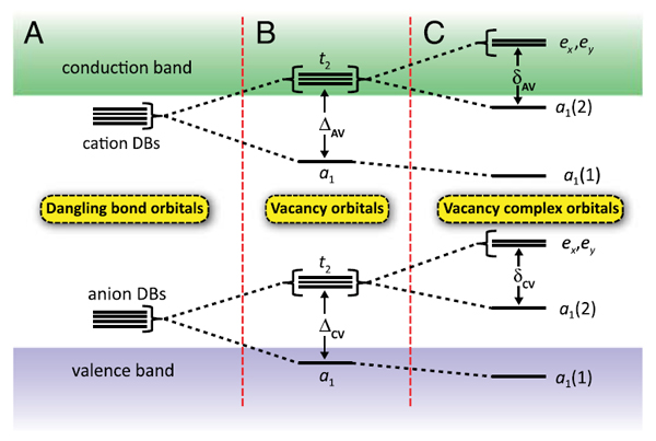
In the diamond NV, the ex, ey, and a1(2) levels are located within the host’s bandgap while the a1(1) level is located in the valence band. Furthermore, the energies of these levels are such that light tuned to 1.945 eV will couple the levels of the diamond NV to one-another, but not to the electronic states of the host (i.e., those at the band edges). Our initial search for NV-like defects includes looking for vacancy-impurity complexes that exhibit analogous level structures, since these will be likely to exhibit similar phenomena to the diamond NV.
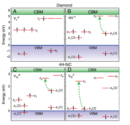
To make more quantitative predictions, computational methods such as Density Functional Theory (DFT) can be exploited. For instance, DFT can be used to predict whether a desired defect is likely to form in a given material, whether the defect will be stable once formed, and how many electrons will be trapped at the defect given the chemical potential (Fermi level) of the surrounding host material. Below we show the results of defect formation energy calculations for various defects in diamond and in the 4H polytype of silicon carbide (4H-SiC). Defect formation energy is a function of the Fermi level in the host material, and the lower the formation energy, the more likely the defect is to form. The dominant charge state for a given defect at a given Fermi level can also be predicted using these plots; it is equal to the slope of the defect’s formation energy at the value of Fermi level specified.

DFT can also be used to make more precise predictions about defect level energies, to predict a defect’s ground-state spin, and to characterize allowed optical excitations in the defect. Below we show calculated predictions of defect level energies for four defects in diamond and 4H-SiC. The conduction band for each material is shown in green, while the valence band is shown in purple. Occupied defect levels are indicated with black arrows, and the dashed green arrows indicate where spin-conserving intra-defect optical transitions should be possible. The energies of these optical transitions can be calculated with further work, providing an initial prediction for the experimentally critical parameter known as the zero-phonon line (ZPL).
Here we have focused on vacancy-related defects and tetrahedrally coordinated semiconductors, but the world of defects is diverse and immense. We hope that the criteria and computational guidelines that have been outlined in this initial work will help to spawn many fruitful collaborations between quantum scientists and materials engineers, leading to a wider exploration of this topic in the future.
For more information, please see: "Quantum computing with defects", J. R. Weber, W. F. Koehl, J. B. Varley, A. Janotti, B. B. Buckley, C. G. Van de Walle, and D. D. Awschalom, Proc. Natl. Acad. Sci. USA 107, 8513 (2010).